ASML and TSMC: High-NA EUV Lithography Contract Extension
ASML has reportedly extended its supply and servicing agreement with TSMC for High-NA EUV lithography machines used in advanced semiconductor manufacturing.
ASML, based in the Netherlands, is the only company producing extreme ultraviolet (EUV) lithography systems. TSMC, headquartered in Taiwan, is the world’s largest dedicated semiconductor contract manufacturer and produces chips for leading technology companies.
The reported agreement highlights the importance of advanced lithography equipment in the development of increasingly powerful and compact semiconductor chips.
What Is High-NA EUV Lithography?
Extreme ultraviolet lithography is a semiconductor manufacturing technology that uses extremely short-wavelength light to print intricate patterns onto silicon wafers. These patterns form the structures needed to manufacture modern processors and other semiconductor components.
High-NA EUV systems represent an advanced development of this technology. The term NA stands for numerical aperture, which describes an optical system’s ability to collect and focus light.
High-NA EUV equipment uses a numerical aperture of 0.55, compared with 0.33 in earlier EUV systems. This improvement enables the printing of finer patterns and supports more advanced chip manufacturing processes.
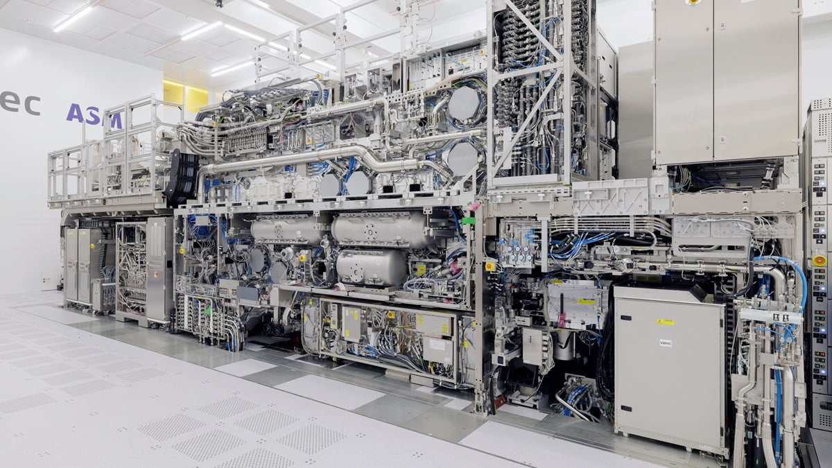
ASML’s High-NA systems belong to the Twinscan EXE series.
ASML and TSMC Contract Details
| Item | Detail |
|---|---|
| Equipment supplier | ASML |
| Supplier headquarters | Netherlands |
| Customer | TSMC |
| Customer headquarters | Taiwan |
| Equipment | High-NA EUV lithography systems |
| Product series | Twinscan EXE |
| Numerical aperture | 0.55 |
| Manufacturing objective | Support for advanced chips, including sub-2nm technology |
| Reported contract value | Not disclosed |
Why High-NA EUV Matters for Advanced Chips
Semiconductor manufacturers are working to produce smaller, more efficient and more powerful chips. Advanced lithography equipment is essential because the patterns printed on silicon wafers determine many of the characteristics of the resulting semiconductor devices.
High-NA EUV technology can help manufacturers print finer features and reduce the need for certain patterning steps. However, adopting the technology also requires substantial investment in equipment, manufacturing processes and supporting infrastructure.
These machines are exceptionally large and complex, with individual systems costing hundreds of millions of dollars. Their installation and operation require specialised facilities and highly trained engineers.
The Importance of ASML and TSMC
ASML’s position in EUV lithography gives the company a central role in the global semiconductor supply chain. Chipmakers depend on its equipment to manufacture some of the world’s most advanced processors.
TSMC’s manufacturing capacity is equally important because its customers rely on the company to produce processors used in smartphones, computers, data centres and artificial intelligence systems.
If the reported agreement improves TSMC’s access to High-NA EUV equipment and servicing, it could influence the company’s long-term advanced manufacturing plans.
The broader significance lies in the competition to manufacture next-generation chips. Access to advanced lithography technology can affect production capabilities, manufacturing costs and the pace at which new semiconductor technologies become available.